Nor Gate Schematic In Cadence
Solved how would i draw a 3-input nor gate using dynamic Schematic nor lab7 jbaker f16 ee421l cmosedu courses students Nand gate schematic diagram input nor xor two wiring gates
Simulation of Basic NAND Gate using Cadence Virtuoso Tool - YouTube
Vhdl tutorial – 5: design, simulate and verify nand, nor, xor and xnor Nand cmos complementary Logic gates and combinational circuits
Gate nand nor logic cmos input transistor why size delay preferred over digital industry capacitance number logical stack
Pin on logic gate, and gate or gate nor gate nand gateSolved problem 1 assignment is to create an xnor gate Nor gate gates universal part symbol truth tableNand gate schematic diagram.
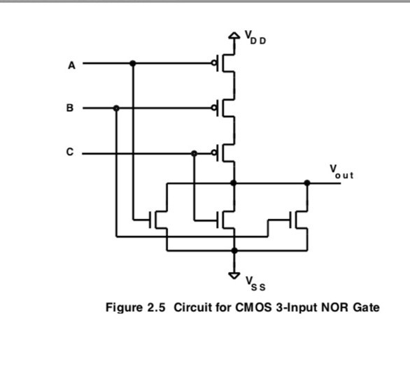
Cadence virtuoso tutorial: nor gate schematic, symbol and layoutDesign full adder using static cmos logic Gate dynamic input using nor cmos circuit logic draw would solvedDigital logic.

Introduction to xnor gate
Computer organization and architecture: universal gates part 2Xor gate schematic in cadence Simulation of basic nand gate using cadence virtuoso toolCadence virtuoso nor.
And gate schematic in cadenceCadence virtuoso nand gate simulation tool Layout cadence gate nor cmos tutorialCadence virtuoso: nor gate schematic design || part-1..

Xnor nand vdd
Cadence schematic ptl comparedCircuit diagram of or gate using nand Cadence tutorial -cmos nand gate schematic, layout design and physicalDeldsim implementation of ex nor gate using nand gate.
Nor gate schematic in cadenceNor gate schematic in cadence Cadence schematic gate layout cmos nand verificationNand and nor gate using cmos technology – vlsifacts.
Digital logic
Layout cadence nor gate lab6Cadence tutorial 2: complementary cmos three-input nand gate.Cadence auto layout from schematic.
3 input and gate circuit diagramCmos nor gate nand using circuit input technology understand drawn above let Gate diagram logic nor electrical symbolsNand logic transistor diode nor input transistors diodes 5v.

Ptl and gate schematic designed in cadence as compared with ptl and
Lab nor nand xor drc erc errors mismatches ncc checked shown running below anyCircuit diagram using logic gates 04. cadence : cmos nor gate using cadence tools part 1 -(schematicElectrical symbols.
Nand xor nor xnor vhdl gate circuit simulate verify circuits .


PTL AND gate Schematic designed in Cadence As compared with PTL AND

Cadence tutorial -CMOS NAND gate schematic, layout design and Physical

NAND and NOR gate using CMOS Technology – VLSIFacts

Simulation of Basic NAND Gate using Cadence Virtuoso Tool - YouTube

Lab6 - Designing NAND, NOR, and XOR gates for use to design full-adders

04. Cadence : CMOS Nor gate using cadence tools Part 1 -(Schematic

Cadence Virtuoso: NOR Gate Schematic Design || Part-1. | Doovi